RESEARCH ARTICLE
An Analytical Theory of Hall-Effect Devices with Three Contacts
Udo Ausserlechner*
Article Information

Identifiers and Pagination:
Year: 2018Volume: 4
First Page: 14
Last Page: 42
Publisher Id: PHY-4-14
DOI: 10.2174/1874843001804010014
Article History:
Received Date: 11/03/2018Revision Received Date: 02/05/2018
Acceptance Date: 22/05/2018
Electronic publication date: 29/06/2018
Collection year: 2018
open-access license: This is an open access article distributed under the terms of the Creative Commons Attribution 4.0 International Public License (CC-BY 4.0), a copy of which is available at: https://creativecommons.org/licenses/by/4.0/legalcode. This license permits unrestricted use, distribution, and reproduction in any medium, provided the original author and source are credited.
Abstract
Object:
Vertical Hall-effect devices (VHalls) and split-drain MAG-FETs often have three contacts and a single mirror symmetry. We discuss the Equivalent Resistor Circuit (ERC) at small magnetic field, relate it to the electrical degrees of freedom, and compare it to traditional Hall plates with four contacts.
Methods:
In contrast to devices with four contacts, it is not possible to determine the sheet resistance of devices with three contacts by electrical measurements like the one of van der Pauw. However, for both types of devices, the output voltage over input current depends only on resistances of the ERC, the sheet resistance, and the Hall angle, irrespective of the exact shape of the devices and the size of the contacts.
Result:
This allows one to explore the maximum Signal-to-Noise Ratio (SNR) in a very general sense without consideration of any specific device geometry. It is shown how VHalls with all three contacts on the top face of the Hall tub can have electrical symmetry with maximum SNR.
1. INTRODUCTION
Traditional Hall plates have four contacts and two perpendicular mirror symmetries [1-4]. Current Iin is sent through two opposite contacts and the output voltage Vout is tapped between the other two opposite contacts (Fig. 1a).
 |
(1) |
with the Hall mobility µH > 0, the magnetic flux density B┴ perpendicular to the thin, plane Hall plate, the sheet resistance Rsh, and the Hall-geometry factor 0< <1. The arctangent of µHB┴ is called the Hall angle. The electrical behaviour of such a 4C-device at zero magnetic field is described by an Equivalent Resistor Circuit (ERC) comprising six resistors with three different resistance values (Fig. 1b) [5]. Irrespective of the size of the contacts, we can use some generalized van der Pauw technique to measure the sheet resistance and the resistances of the ERC [5]. From the ERC, we can compute the input resistance Rin between the supply contacts and the output resistance Rout between the sense contacts. Thereby, the ratios of input and output resistances over sheet resistance Rin / Rsh, Rout / Rsh depend only on the lateral geometry of the Hall plate, i.e., its layout. We call them the effective numbers of squares of input and output resistances λin, λout.
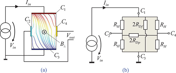 |
Fig. (1). (a) Traditional 4C-Hall-plate with current streamlines at strong magnetic field µHB┴ = 1 pointing out of the drawing plane. (b) Equivalent Resistor Circuit (ERC) of the same Hall plate at zero magnetic field. |
 |
(2a) |
 |
(2b) |
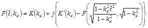
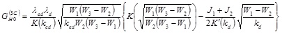
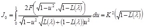
Together with the sheet resistance these 3 DoF fully characterize the electrical behaviour of the Hall plate at zero magnetic field. Moreover, they also describe the behaviour of the Hall plate at arbitrary magnetic field. For small magnetic field, we even know an analytical relation [6]:
 |
(3) |
with the incomplete elliptic integral of the first kind 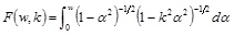 , the complete elliptic integral of the first kind K(k) = F (1, k), the complementary elliptic integral
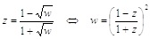
  , and the modular lambda function L(y), defined by L(K'(k) / K(k)) = k2 for 0 ≤ k ≤ 1 [5]. There is a non-trivial symmetry
  [6].
[6].
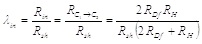
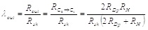
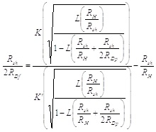
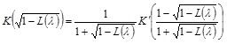
In modern times, Hall plates are mostly operated in the spinning current Hall probe scheme, which reduces the offset error by 2 ½ decades (in silicon technology from 5 mT initial offset to 10 µT residual offset) [7, 8]. The scheme comprises various operating phases where the supply and sense contacts of the Hall plate are swapped (contact commutation). An appropriate sum or difference of output signals of individual operating phases cancels out offset errors while boosting the magnetic sensitivity. It also cancels out flicker noise, if the spinning frequency is chosen larger than twice the flicker noise corner frequency [9]. For this scheme, it is convenient to use Hall plates with equal input and output resistances Rin = Rout or λin = λout. This can be readily done with layouts of 90° symmetry. The ERC has only two resistance values for the six resistors, because in Fig.(1b) we simply have to set RDf = RDP → RD. Then the generalized van der Pauw measurement has a simpler formula for λin = λout → λ and Rsh (see (26) in [10]). The 2 DoF λ, Rsh are linked to the ERC via
 |
(4a) |
 |
(4b) |
with  [10, 11]. In (4a,b) the minus-sign is used for
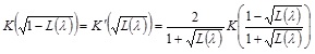
  and the plus-sign in the opposite case. The accuracy of (4a,b) is +/-0.02%. Again the number of squares λ depends only on the layout, and it fully determines the Hall-geometry factor at small magnetic field [12]
 |
(5a) |
 |
(5b) |
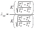
with  and c0 = 2.279, c2 = 1.394, c4 = 0.6699, c6 = 0.4543. The accuracy of (5a) is -2%/+0%, and the accuracy of (5b) is -60ppm/+0.02%. Here the symmetry is between complementary devices
  Fig. (8) in [6]).
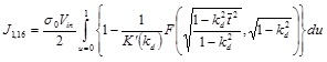
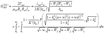
With these results, one can show that the ratio of the output signal over thermal noise is given by [6]
 |
(6) |
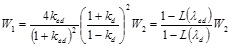
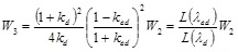
with Boltzmann’s constant kb, the absolute temperature T, the effective noise bandwidth Δf, and the available Hall supply voltage VH sup = IinRin. At a given impedance Rin the SNR gets largest for symmetric devices with [6]
 |
(7) |
Hence, in silicon technology at room temperature, a 500 Ω device operated at 2.5 V supply can achieve a maximum magnetic resolution of 566 nT in 1 kHz noise-equivalent bandwidth [6]. This Hall plate needs to be quite thick (~45 µm) – alternatively one may connect 45 devices with 1 µm thickness in parallel (which can be accommodated in 150 µm x 150 µm chip area).
Recently, vertical Hall-effect devices (VHalls) have been attracting significant attention from the industry, because they allow one to measure the in-plane magnetic field components, i.e. the magnetic field components parallel to the chip surface (Bx, By), whereas Hall plates – also called horizontal Hall-effect devices (HHalls) – respond to the magnetic field component orthogonal to the chip surface (Bz) [13, 14]. A vast plurality of topologies was proposed for VHalls, yet one important group of VHalls comprises a single Hall tub with only three contacts on one side and a single mirror symmetry Fig. (2) [15, 16]. It can also be viewed as a basic building block for more complex Hall-effect devices. Besides, this type of symmetry also applies to split-drain MAG-FETs [17]. Therefore, we are interested in a theory of such devices analogous to the foregoing one for 4C-devices. And indeed, we will find many analogies and a few distinct differences between devices with 3 and 4 contacts.
 |
Fig. (2). Vertical Hall-effect device with three contacts and a single mirror symmetry. |
2. THE DEGREES OF FREEDOM AND THE EQUIVALENT RESISTOR CIRCUIT
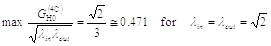
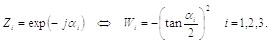
Fig. (3a) shows a plane circular disk-shaped device without holes and with three arbitrary contacts on its perimeter. Obviously, its layout has 7 geometrical degrees of freedom α1, α2, ...α6 plus the diameter, but we can scale the diameter to 1 and rotate the device so that α6 → 0 without affecting its electrical properties, and then we end up with 5 DoF. We can further map the interior of the disk in the z -plane onto the upper half of the w' -plane by a Möbius transformation w' = (a1 + a2z) / (1 + a3z) with 3 complex-valued parameters a1, a2, a3, which we are free to choose except for a2 ≠ a1a3 [18]. Thus, from the 6 points Z1, Z2, ...Z6 we can map 3 points at fixed positions in the w' -plane: in Fig. (3b) we map Z1 = exp (- jα1) → W1' = 0, Z2 = exp (- jα2) → W2' = –1, Z6 = exp (- jα6) → W6' = 1 with  [19], so that only 3 points W3', W4', W5' on the real axis of the w' -plane are free to describe the specific contact geometry. These 3 scalar parameters plus the sheet resistance give 4 electrical DoF, which fully describe the electrical behaviour of the device. On the other hand, we know from linear circuit theory that a resistive network with three terminals can be represented by its ERC, which has a resistor between each pair of contacts. This gives only 2+1 = 3 resistors Fig. (3c). Hence, we have 4 DoF W3', W4', W5', Rsh in the w' -plane, which are mapped to just 3 DoF Ra, Rb, Rc in the ERC! In other words, for a given ERC we can freely choose one of the 4 DoF in the w' -plane. For example, we could choose a value for the sheet resistance and select appropriate three parameters W3', W4', W5' to achieve any required ERC. Therefore, it is impossible to determine the sheet resistance from electrical measurements on a 3C-device at zero magnetic field.
 |
Fig. (3). (a) Asymmetric 3C-HHall. (b) Its conformal transformation on the upper half of the w' -plane has 4 electrical DoF W3', W4', W5', Rsh. (c) Its ERC has only 3 electrical DoF Ra, Rb, Rc . |
Next we increase the symmetry according to Fig. (4a), where the contacts exhibit one symmetry axis. This is the type of device which we focus on in the main part of this work. After rotation into a favourable position the layout is described by 3 DoF in the z -plane α1, α2, α3. The Möbius-transformation w' = (1 + exp(iα2))(1 - exp(iα2))-1(1 - z)(1 + z)-1 reduces the number of scalar parameters to two, namely
 |
(8a) |
 |
(8b) |
Fig. (4b). With the sheet resistance this gives 3 DoF (k12, k23, Rsh), however, the ERC has only two resistance values (Rd, Re). Again we may freely choose one out of k12, k23, Rsh to obtain any given ERC.
Finally, we increase the symmetry even further according to Fig. (5a). Now the device has a 120° symmetry and the layout in the z -plane has only one scalar parameter θ that affects the electrical behavior. After a Möbius-transformation the layout in the w' -plane has still one scalar parameter 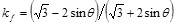 . The second parameter is not free – it follows from the first one
  . With the sheet resistance we have 2 electrical DoF, but the ERC has only a single resistance value (Fig. 5c). Thus, for a given electrical behaviour at zero magnetic field we can choose any arbitrary value for Rsh and select kf according to the following equation.
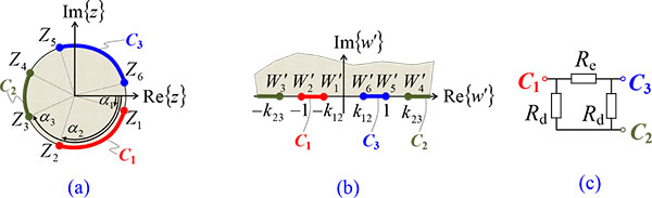 |
Fig. (4). (a) 3C-HHall with a single mirror symmetry axis Re{z}. (b) Its conformal transformation on the upper half of the w' -plane has 3 electrical DoF k12, k23, Rsh. (c) Its ERC has only 2 electrical DoF Rd, Re . |
 |
Fig. (5). (a) Symmetrical 3C-HHall. (b) Its conformal transformation on the upper half of the w' -plane has 2 electrical DoF kf, Rsh (κ f is a function of k f ). (c) Its ERC has only 1 electrical DoF Rf . |
 |
(9) |
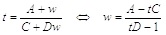
How does this look like with conventional 4C-devices? For 90° symmetry the layout has 1 DoF (Fig. 6a). Adding the sheet resistance gives 2 DoF describing its electrical behavior at zero magnetic field. The ERC of a device with four contacts has 3+2+1 = 6 resistors, but with the high symmetry we have only two resistance values RH, 2RD Fig. (6c) [10]. These two resistances and the sheet resistance are not independent from each other. From [10] we use (14) and (15) into (5a) and we use (A15) from [5] to get L(4Rsh / RH) = k12 with k1 = (1 - tan α1) / (1 + tan α1). Again from [10] we plug (14) into (4b) to get Rsh(1 / RH + 1 / (2RD)) = K'(k1) / (2K(k1)). Combining both we get:
 |
Fig. (6). (a) 4C-HHall with 90° symmetry. (b) Its conformal transformation w' = -j cot(π/8 + α1/2)(z - exp(jπ/4))/(z + exp(jπ/4)) has 2 electrical DoF, because W'1 = tan(π/8 - α1/2)/ tan(π/8 + α1/2), W'3 = cot2(π/8 + α1/2), and W'4 = cot(π/8 - α1/2) cot(π/8 + α1/2) are linked to a single DoF α1 and the sheet resistance Rsh is the second electrical DoF. (c) Its ERC has also 2 electrical DoF. |
 |
(10a) |
Therefore, RH / Rsh and RD / Rsh represent only a single DoF, and the 2 DoF of the ERC are covered by RH / Rsh and Rsh. The reason, why we can measure sheet resistance with van der Pauw technique is: the ratio RH / RD is accessible to electrical measurement and it depends only on the layout and not on the sheet resistance. From (6), (14), (15) in [10] and (A15) in [5] we derive the relation
 |
(10b) |
with λ = 2K(k1) / K'(k1). (10b) rises monotonously from 0 to 1 for λ: 0 → ∞. Hence, from electrical measurements, we can uniquely infer the number of squares λ and with this information, we get the sheet resistance.
If we reduce the symmetry according to Fig. (7a) the device has two orthogonal mirror symmetries and thus different input and output resistances. This gives 3 electrical DoF λin, λout, Rsh (see (2a,b)). The ERC has three resistance values RH, RDf, RDp which are related via the sheet resistance: From [5] we use (1a) to express Rsh(1 / RH + 1 / (2RDf)), and then we insert (1b) and (2c) of [5] into (A14) of [5]. Combining both results we can express RDf / Rsf as a function of RDp / Rsh and RH / Rsh:
 |
(11) |
Consequently, the 3 electrical DoF can be represented by RDp / Rsh, RH / Rsh, Rsh.
We skip the discussion of 4C-devices with 4 and 5 DoF and conclude with the case of entirely asymmetric devices. The 4 contacts are defined by 8 arbitrary end-points, 3 of which we can map via Möbius-transformation onto defined points on the Re {w'}-axis. This gives 5 DoF of the layout plus the sheet resistance. So we end up with 6 electrical DoF, which matches the 6 resistances in the ERC [8]. If we normalize these 6 resistances in the ERC by the sheet resistance, there must be one relation between them: the 6th one follows out of the first 5 ones. In a weaker form this has already been mentioned in the appendix of the seminal paper by Van der Pauw [20].
 |
Fig. (7). (a) 4C-HHall with two perpendicular mirror symmetries has 3 electrical DoF α1, α2, Rsh. (b) Its conformal transformation on the upper half of the w' -plane. (c) Its ERC has also 3 electrical DoF. |
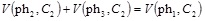
To sum up, in this section, we have shown two remarkable differences between 3C- and 4C-devices: (1) from mere electrical measurements on a 3C-device and without knowledge of the device geometry one cannot deduce the sheet resistance, however, for 4C-devices this works irrespective of the size of the contacts. (2) for a fixed shape of the Hall-effect region and a fixed ERC (i.e. fixed electrical behavior) there is exactly one contact geometry and one sheet resistance in the case of 4C-devices, however, in the case of 3C-devices we will find infinitely many contact geometries and sheet resistances (whereby we assume plane devices, simply connected region, homogeneous and isotropic conductivity, constant thickness, and the contacts must be at the perimeter).
3. THE ERC OF A 3C-DEVICE WITH SINGLE MIRROR SYMMETRY
Here we compute the two resistances Rd, Re of the device from Fig. (4a). Thereby, we look for operating conditions with symmetric potential distributions at zero magnetic field, which can be generated by only two contacts, because this leads to comparably simple, closed-form conformal transformations in terms of elliptic integrals.
3.1. Current Flow Across the Line of Mirror Symmetry
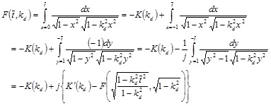
In Fig. (4a) the Re{z}-axis is the line of mirror symmetry. If we connect C1 to +1V and C3 to -1V, C2 and the Re{z}-axis will be at 0V and we need to study only the potential distribution in the lower half of the device with the two contacts C1, C2. Fig. (8) shows a sequence of conformal transformations, which map the semi-circular region onto a rectangle, with the contacts at opposite sides, so that we immediately know the resistance between them. The first transformation is [21]:
 |
(12a) |
which maps Z34 = -1 → W34 = -∞, Z 0 = 0 → W 0 = 1, Z16 = 1 → W16 = 0, . For the essential points that define the contacts we get
 |
(12b) |
Valid ranges are 0 < αi <π, -∞ < Wi < 0 for i = 1,2,3. The w-plane in Fig. (8b) and the w' -plane in Fig. (4b) differ only in an isotropic scaling factor w = (tan (α2 / 2))2w'. We symmetrize the contacts by the Möbius transformation:
 |
(13a) |
 |
(13b) |
 |
(13c) |
 |
(13d) |
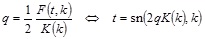
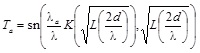
With 0 < α1 < α2 < α3 it follows W3 < W2 < W1 < 0 from which follows 0 < ked < 1. A final Schwartz-Christoffel transformation maps the upper half of the t-plane onto the interior of a rectangle in the q-plane (see also Fig. (3d) in [22]).
 |
(14a) |
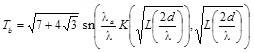
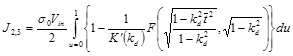
sn(F(t, k), k)=t is the Jacobi sine-amplitude function. The aspect ratio of the rectangle gives the resistance between C1 and C2 in this operating mode
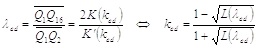 |
(14b) |
For the R.H.S. of (14b) we used (A18) in [5].λed is strictly monotonously rising versus ked.
 |
Fig. (8). (a-d) Sequence of transformations that map the lower half of a circular device with current flow across its axis of single mirror symmetry onto a rectangle z → w → t → q with homogeneous current density. |
3.2. Current Flow Along the Line of Mirror Symmetry
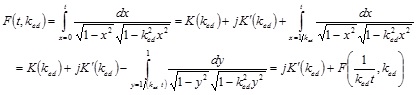
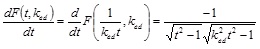
If we connect C1 and C3 to +1V and C2 to 0V in Fig. (4a), we get a second symmetrical potential distribution. Fig. (9) shows a sequence of conformal transformations, which map the semi-circular region onto a new rectangle, that is different from the rectangle in Fig. (8d), because the line of symmetry is not on constant potential anymore. The first transformation z → w is identical to (12a), but the Möbius transformation is different.
 |
(15a) |
 |
(15b) |
 |
(15c) |
 |
(15d) |
 |
Fig. (9).
(a-d) Sequence of transformations that map the lower half of a circular device with current flow along its axis of single mirror symmetry onto a rectangle z → w →  → →  with homogeneous current density. with homogeneous current density.
|
With W3 < W2 < W1 < 0 it follows 0 < kd < 1. A final Schwartz-Christoffel transformation maps the upper half of the  -plane onto the interior of a rectangle in the
  -plane.
 |
(16a) |
The aspect ratio of the rectangle gives the resistance between C1 and C2
 |
(16b) |
For the R.H.S. of (16b) we used (A19) in [5].λd is strictly monotonously falling versus kd.
3.3. The ERC and its Properties
Comparison of (14b) with the ERC in Fig. 4c gives
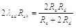 |
(17a) |
Comparison of (16b) with the ERC in Fig. 4c gives
 |
(17b) |
Solving (17a,b) for the two resistances of the ERC gives
 |
(18a) |
 |
(18b) |
Since Rd, Re fully define the electrical behaviour of the device, (17a,b) imply that Rshλd, Rshλed also describe the 2 electrical DoF. Thus, Rshλd and Rshλed are independent of each other, and therefore λd and λed are also independent of each other. Analogous to (18a) we can define
 |
(18c) |
so that any single one of the parameters λd, λed, λe can be expressed by the other two.
On the other hand, we can invert (13d) and (15d) to express two parameters out of W1, W2, W3 by kd, ked or by λd, λed.
 |
(19a) |
 |
(19b) |
We can obtain any arbitrary ERC by picking some arbitrary value for W2: then W1 and W3follow from (19a,b). In particular, we may choose W2 = -1. Then we can model all possible ERCs by W1 (-1,0) and W3 (-∞, -1). Thus, we have reduced the problem in three dimensions to a problem in two dimensions. Alternatively, we may also write
 |
(19c) |
 |
(19d) |
(19c,d) tell us how to choose W1, W2 – i.e. location and size of contact C1 – so that we can obtain any arbitrary ERC with α3, i.e. with a fixed size of contact C2 (the location of C2 is given by symmetry). This has an important application for VHalls with three contacts: we can choose any convenient size for the center contact C2 – by playing around with location and size of the outer contacts we still have all 2 DoF at our option.
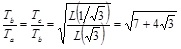
From W3 < W2 < 0 we get with (19a,b) or (19c,d) L(λd) < L(λed) and finally
 |
(20a) |
With (18b) this means Re > 0. With the L.H.S. of (14b), (16b) and with (28) in [22] this also means
 |
(20b) |
 |
(20c) |
which limits the allowed region in (kd, ked) –space to a narrow region.
A device with a geometrical symmetry of 120° has α2 = (2π / 3) - α1 and α3 = (2π / 3) + α1. Since the gap between contacts must be smaller than 120° the valid ranges are 0 < α1 < π / 3 which is equivalent to -1/3 < W1 < 0. It holds  with -3 < W2 < -1/3 and
  with -∞ ≤ W3 ≤ -3. Since this device must also have electrical symmetry, the ERC leads to Rd = Re. With (18a,b,c) it follows λd = λe = 3λed.
A device without geometrical symmetry may still have electrical symmetry Rd = Re with λd = λe = 3λed. With (14b), (16b) this means K'(kd) / K(kd) = 12K(ked) / K'(ked). This modular equation of degree 12 can be solved in two steps by K'(k) / K(k) = 3K'(l) / K(l) and K'(l) / K(l) = 4K(m) / K'(m). The solution of the first equation of degree 3 is given by (13) in [23]  , and the second one by (28) in [22]
  . With (13d), (15d) this gives an implicit function f(α1, α2, α3) = 0, which is plotted in Fig. (10). For comparison, the solid black line in the plot denotes devices with 120° symmetry. Obviously, there are many circular devices which have only electrical symmetry and no geometrical 120° symmetry.
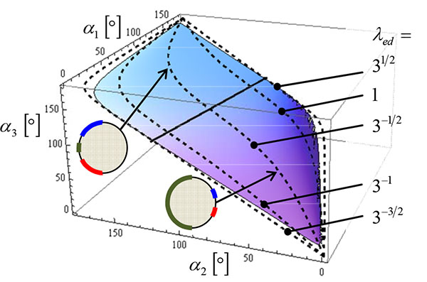 |
Fig. (10).
All possible parameter-sets α1, α2, α3 for circular 3C-devices with single mirror symmetry from Fig. (4), that have electrical symmetry Rd = Re. The straight solid black line denotes devices with geometrical 120°-symmetry. The rest of the surface denotes devices without geometrical symmetry but with electrical symmetry. The surface is symmetric: each device right of this line has a complementary device left of this line where contacts and isolating boundaries are swapped. Two examples of such devices are shown and their respective locations on the surface are indicated. The dashed lines denote devices with constant λed and λd and thus identical  (i.e. constant Hall output signal at fixed supply current, see (31)). (i.e. constant Hall output signal at fixed supply current, see (31)).
|
In the limit of point-sized contacts we set α2 → α1 + 2δ and α3 → π – δ with δ → 0. From (12b) we get  and W3 → -4 / δ2. From (13d), (15d) we get
 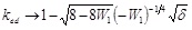 and
and 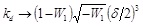 . With (14b), (16b) we get λed → ∞, λd → ∞ and
 |
(21) |
where we used K (0) = π / 2 and 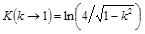 . Thus, the limit of point-sized contacts at arbitrary location is identical with the limit of point-sized contacts at 120° symmetry.
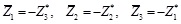
If we swap isolating boundaries with contacts in Fig. (4a) we obtain the complementary device, which has also three contacts and a single mirror symmetry (see Figs. (11a, b)). Denoting the parameters of the complementary device by an overbar and the conjugate complex by an asterisk, we get the following relations.
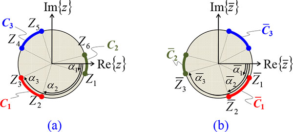 |
Fig. (11). (a) 3C-HHall with a single mirror symmetry axis Re{z} obtained from Fig. (4a) by swapping contacts and isolating boundaries. (b) Device obtained from (a) by mirroring on the imaginary axis. |
 |
(22a) |
 |
(22b) |
 |
(22c) |
 |
(22d) |
 |
(22e) |
 |
(22f) |
If a device has electrical symmetry λd = 3λed, then also its complementary device has electrical symmetry  .
.
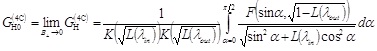
4. THE MAGNETIC SENSITIVITY OF A 3C-DEVICE WITH SINGLE MIRROR SYMMETRY
A 3C-Hall-effect device can be operated in various operating modes (see Fig. (6) in [19]). For each operating mode one can find a spinning current scheme that cancels out offset errors perfectly, as long as the device is assumed to have electrical linearity1. First we show that even though the 3C-device may be entirely asymmetric like in Fig. (3), its
1 Electrical linearity means that the resistance values in the ERC do not depend on the potentials at the various nodes. However, the device may be magnetically nonlinear, which means that the resistance values in the ERC may well depend on the applied magnetic field – so we do not have to limit this discussion to small magnetic fields.
current related magnetic sensitivity Si = (1 / Iin) ∂Vout / ∂B┴ is identical in all operating phases of a spinning current scheme. Then we use this finding to compute the Hall-geometry factor for devices with single mirror symmetry.
4.1. The Hall-Geometry Factor in All Spinning Phases of a 3C-Device
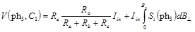
We use the principle of superposition as introduced in [24]. Let us consider an asymmetric VHall device with three contacts. In a first operating phase ph1 the device is supplied at its outer contacts (see Fig. (12a) and the ERC in Fig. (12b). We can use the ERC to compute the potentials and currents at the contacts of the device but we have to add an extra Hall term  whenever a contact is left of the current flow through the device (and we subtract it, when the contact is right of the current flow2). We can think of two further operating phases ph2 and ph3, where the current flows between an outer contact and the mid-contact. Phases ph2 and ph3 are chosen such that their superposition gives phase ph1 (see Fig. 12c-12f). This means that the sum of currents into each contact in phases ph2 and ph3 must equal the current into the respective contact in phase ph1, and the sum of potentials at each contact in ph2 and ph3 must also equal the potential at the respective contact in ph1 [25]. With linear circuit theory we get the following potentials at contact C1.
 |
Fig. (12).
(a, c, e) Asymmetric 3C-VHall in operating phases ph1, ph2, ph3. (b, d, f) Its respective ERCs. The dashed lines in (a, c, e) denote the global current flow in the Hall-effect regions. The potentials at the contacts are computed by the ERCs in (b,d,f) and the extra terms  shown in (a, c, e), which have to be added to the potentials at the indicated contacts to account for the Hall effect. shown in (a, c, e), which have to be added to the potentials at the indicated contacts to account for the Hall effect.
|
 |
(23a) |
 |
(23b) |
 |
(23c) |
Note that in ph3 the Hall action of the VHall device tries to reduce the potential at C3 by 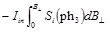 , but the ground wire ties C3 to 0 V thereby lifting all other potentials in the device by
 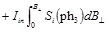 . Superposition of ph2 and ph3 gives ph1:
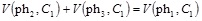 |
(23d) |
Inserting (23a-c) into (23d) gives 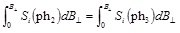 . Since this is valid for all B┴ we can differentiate the equation with respect to B┴ and it follows Si(ph2) = Si(ph3). We repeat the same for contact C2.
 |
(24a) |
 |
(24b) |
 |
(24c) |
 |
(24d) |
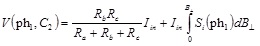
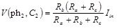
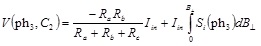
With (24a-d) it follows Si(ph1) = Si(ph3). Hence, the current related magnetic sensitivity Si is equal in all phases ph1, ph2, ph3. This holds for 3C-devices with and without symmetry. Thereby the magnetic field may even be strong, so that the resistances Ra, Rb. Rc and the current related magnetic sensitivity Si become nonlinear functions of B┴ – the principle of superposition requires only electrical linearity, not magnetic linearity. According to [19] we can define the Hall-geometry factor of 3C-Hall-effect devices by
 |
(25) |
with  . Thus,
  is constant for all phases ph1, ph2, ph3, too. If we know and the ERC, we know the Hall output signals in all operating conditions.
4.2. The Weak Field Hall-Geometry Factor of a 3C-Device with Singe Mirror Symmetry
For small Hall angles one can use a perturbation approach, where the potential in the Hall-effect region is developed into powers of µHB┴ and only the lowest order term is used to compute the Hall output signal [26, 27]. The procedure is developed in detail in [22]: In a first step we compute the potential at zero magnetic field. Thereof, we get the electric field Ep along the isolating boundaries. However, in the presence of a magnetic field, the Hall effect gives rise to an additional component of the electric field, which is normal to the isolating boundary En = µhB┴Ep with the Hall angle 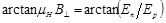 . We take account of the component En in a second step, where we tie all supply contacts to zero potential, and impose a perpendicular current density on the isolating boundaries Jn = σ 0En, with σ 0 being the conductivity at zero magnetic field. As in the first step also in this second step we use the isotropic conductivity σ 0 throughout the Hall-effect region. The output contacts are at unknown potential Vout and – depending on biasing conditions – usually no net current is flowing in or out of them. Solving the net current condition at the output contacts returns Vout proportional to µhB┴. The advantage of this method is that we can use symmetries of the device, whereas in the case of strong magnetic field these symmetries get lost. Another asset is that in the course of this calculation we can re-use conformal mappings of the ERC-computation in section 3.
From section 4.1 we know that the Hall-geometry factor is identical in all operating phases. So we choose current flow from contact C1 to C3 in a circular device with single mirror symmetry of Fig. (8), because it gives highly symmetric current flow lines. In step 1 this will give us the inhomogeneous electric field along the isolating boundaries  and
and  in the z-plane in Fig. (8a), or along
  and
and  in the w-plane in Fig. (8b). In the q-plane in Fig. (8d) this electric field is simple to compute and homogeneous. It becomes inhomogeneous via the transformations q → t → w. For step 2 we look at the complete original device in Fig. (4) with its symmetry. There we note that with C1 and C3 at zero volts and the current Jn imposed on all isolating boundaries the current flow of the Hall reaction will not flow across the real axis. So we can use the lower semi-circular region of Fig. (9a) to compute the Hall output voltage Vout. It is easier to use the w-plane in Fig. (9b), where we already have an expression for Jn in the intervals
  and
and  from step 1. We can transform this current via w → → onto the rectangle in Fig. (9d), where Jn is impressed on the boundaries
  and
and  . To sum up: the homogeneous current Jp along the isolating boundary in the q-plane is transformed into the -plane via q → t → w → → where it defines the boundary condition Jn = µHB┴Jp on parts of the isolating boundary. The solution of the potential in the -plane finally gives the Hall output voltage.
Similar to [22] we make the ansatz
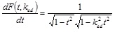
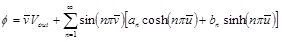 |
(26) |
for the potential in the -plane of Fig. (9d), whereby  . This satisfies two boundary conditions
  and
and 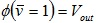 where Vout is the change in potential at contact C2 caused by the action of the small magnetic field. The net current into the output contact must vanish. Thus,
 |
(27a) |
(26) in (27a) and integration gives
 |
(27b) |
The boundary conditions on the left and on the right edge of the rectangle in the -plane are
 |
(28a) |
 |
(28b) |
 |
(28c) |
Positive Jn on the left edge  = 0 means that current flows into the Hall-effect region, whereas positive Jn on the right edge = 1/λd means that current flows out of the Hall-effect region. Introducing the ansatz (26) into (28a-c) and making a Fourier series expansion gives the unknown coefficients an, bn in (27b)
 |
(29a) |
 |
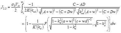
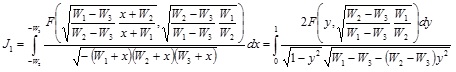
(29b) |
We insert (29a,b) into (27b), use Jn = µHB┴Jp, and reverse the sequence of summation and integration, thereby using  .
.
 |
(30) |
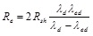
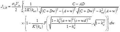
In (30) we only have to determine the transformation of current density from q-plane in Fig. (8d) to -plane in Fig. (9d), which is detailed in Appendix A. The subtraction in (30) means that the current flowing along the boundary between the supply contacts C1 and C3 reduces the Hall output signal. Finally, the weak magnetic field limit of the geometry factor of a 3C-Hall-effect device with single mirror symmetry is given by
 |
(31) |
with the abbreviations Ld = L(λd), Led = L(λed). Equation (31) is the core result of this work. It is valid for any operation mode, where current Iin flows into one contact and out of another contact and voltage Vout is tapped at the third contact. λd, λed are the 2 DoF of the layout and with (17a,b) they can be expressed by ratios of resistances of the ERC over the sheet resistance. Thus, (31) gives the low field limit of the Hall-geometry factor as a function of purely electrical parameters Rd / Rsh, Re / Rsh, irrespective of the geometry of the device.
4.3. Discussion of Magnetic Sensitivity and SNR of 3C-Devices
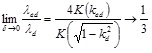
With numerical integration it is straightforward to plot versus its 2 DoF in the allowed region 0 ≤ λed ≤ λd (cf. (20a)) as shown in Fig. (13). There the black solid curve on the surface represents for electrically symmetric devices with Rd = Re which means λd = λe = 3λed. Obviously, → 0 for small λd, λed, i.e. large contacts. On the other hand, with (21) we know that for point-sized contacts at arbitrary position we are located at the far end of the black solid curve. There → 1 [19]. If we plot the points on the black solid curve versus λed we get the same plot as in Fig. (18) of [19]. Hence, our analytical formula (31) is consistent with results from numerical simulations on 120° symmetric 3C-HHalls. Interestingly, in Fig. (13a) the black solid curve does not lie on the crest of the surface: for fixed λd the function has its maximum for λed > λd / 3, thus, not for symmetric devices. At fixed λd the function goes to zero for small λed (which means that the spacing between contacts C1 and C2 gets small) and for λed → λd (which means that contacts C1 and C3 get small while C2 remains finite) (see Appendix B).
Similar to 4C-devices, we note also for 3C-devices a symmetry of the Hall-geometry factor. For devices with electrical symmetry λd = 3λed numerical inspection suggests the following conjecture3
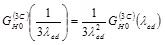 |
(32) |
The physical significance is also the same: it links the Hall geometry factor (λed) of a device with the Hall geometry factor of its complementary device 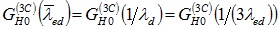 from (22e). Therefore we only need to know the Hall geometry factor for small contacts with
  because we can obtain its values for large contacts with the above symmetry relation. A simple approximation is
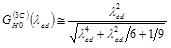 |
(33) |
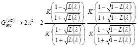
with an accuracy of -2.3%/+1.7%. In [19] we showed that at a given impedance level the signal-to-noise ratio (SNR) of a 3C-Hall-effect device is proportional to 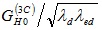 . This parameter is plotted in Fig. (14) for all possible devices. Similar to 4C-devices we note a clear maximum and this maximum occurs for devices with electrical symmetry:
  for
for  and
and  . Such devices with circular shape may have various contact sizes, such as α1 = 30o, α2 = 90o, α3 = 150o, or α1 = 1.1o, α2 = 4o, α3 = 15o, or α1 = 8.2o, α2 = 30o, α3 = 90o, or α1 = 57.2o, α2 = 127.7o, α3 = 165o (see Table 1 and [19]).
 |
Fig. (13).
The weak-field Hall-geometry factor of devices with three contacts and a single mirror symmetry versus its 2 DoF of the layout. In (a) the 2 DoF are λed, λd in (b) the 2 DoF are the resistances of the ERC normalized to the sheet resistance Rd/Rsh, Re/Rsh and in (c) the 2 DoF are the resistances between two contacts normalized to the sheet resistance RC1 → C2/Rsh, RC1 → C3/Rsh. The black solid curves denote devices with electrical symmetry Rd = Re (i.e.λd = λe = 3λed and RC1 → C2 = RC1 → C3). Re 2Rd means the parallel connection of Re and 2Rd. 2Rd means the parallel connection of Re and 2Rd.
|
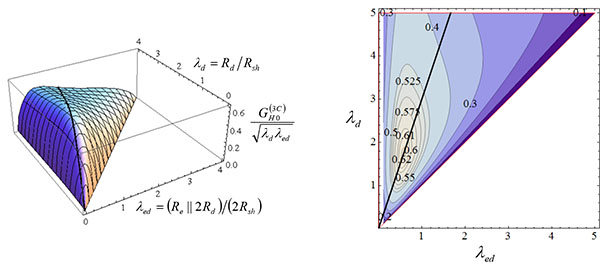 |
Fig. (14). for all 3C-devices with single mirror symmetry versus its 2 DoF λd, λed. The black solid curve denotes devices with electrical symmetry Rd = Re (i.e.λd = λe = 3λed). This curve goes right over the peak of the surface at 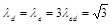 with with 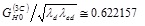 . .
|
. These three layouts are defined by α3 = 15o, 90o, 165o according to (19c,d).| α3 = 15° | α3 = 90° | α3 = 165° | ||||||||||
|---|---|---|---|---|---|---|---|---|---|---|---|---|
| n | m | λd | λed | λed/ λd | GH0(3C) | GH0(3C)/sqrt(λedλd) | α1 [°] | α2 [°] | α1 [°] | α2 [°] | α1 [°] | α2 [°] |
| -6 | -13 | 0.1925 | 0.0111 | 0.0575 | 0.00213 | 0.046138176862 | 1.121E-57 | 14.99999 | 8.512E-57 | 89.99996 | 6.465E-56 | 164.9999 |
| -4 | -13 | 0.3333 | 0.0192 | 0.0575 | 0.00639 | 0.079903222319 | 4.145E-33 | 14.99043 | 3.149E-32 | 89.96301 | 2.392E-31 | 164.9904 |
| -2 | -13 | 0.5774 | 0.0332 | 0.0575 | 0.01902 | 0.137442192251 | 6.232E-19 | 14.49442 | 4.734E-18 | 88.01405 | 3.596E-17 | 164.4772 |
| 0 | -13 | 1.0000 | 0.0575 | 0.0575 | 0.05346 | 0.222973608073 | 8.156E-11 | 10.63694 | 6.195E-10 | 70.52878 | 4.706E-09 | 158.9063 |
| 2 | -13 | 1.7321 | 0.0996 | 0.0575 | 0.12790 | 0.308008961734 | 2.27E-06 | 3.903103 | 3.149E-32 | 29.02164 | 0.000131 | 126.0782 |
| 4 | -13 | 3.0000 | 0.1724 | 0.0575 | 0.25100 | 0.348986748377 | 0.00024 | 0.541918 | 0.001822 | 4.11454 | 0.013837 | 30.52348 |
| 6 | -13 | 5.1962 | 0.2987 | 0.0575 | 0.43819 | 0.351752517952 | 0.000358 | 0.017218 | 0.002719 | 0.130783 | 0.02065 | 0.993374 |
| -6 | -11 | 0.1925 | 0.0172 | 0.0892 | 0.00330 | 0.057475754415 | 9.573E-36 | 14.99999 | 7.272E-35 | 89.99996 | 5.523E-34 | 164.9999 |
| -4 | -11 | 0.3333 | 0.0297 | 0.0892 | 0.00991 | 0.099537916218 | 1.905E-20 | 14.99043 | 1.447E-19 | 89.96301 | 1.099E-18 | 164.9904 |
| -2 | -11 | 0.5774 | 0.0515 | 0.0892 | 0.02952 | 0.171215991296 | 1.274E-11 | 14.49442 | 9.677E-11 | 88.01405 | 7.350E-10 | 164.4772 |
| 0 | -11 | 1.0000 | 0.0892 | 0.0892 | 0.08296 | 0.277765096227 | 1.356E-06 | 10.63694 | 1.03E-05 | 70.52878 | 7.823E-05 | 158.9063 |
| 2 | -11 | 1.7321 | 0.1545 | 0.0892 | 0.19846 | 0.383658608695 | 0.000621 | 3.903103 | 0.004715 | 29.02164 | 0.035812 | 126.0782 |
| 4 | -11 | 3.0000 | 0.2676 | 0.0892 | 0.38717 | 0.432124790103 | 0.006121 | 0.541953 | 0.046494 | 4.114801 | 0.353153 | 30.52533 |
| 6 | -11 | 5.1962 | 0.4635 | 0.0892 | 0.63874 | 0.411599637973 | 0.002333 | 0.017372 | 0.017724 | 0.131951 | 0.134627 | 1.002241 |
| -6 | -9 | 0.1925 | 0.0266 | 0.1384 | 0.00513 | 0.071599325552 | 1.299E-21 | 14.99999 | 9.868E-21 | 89.99996 | 7.495E-20 | 164.9999 |
| -4 | -9 | 0.3333 | 0.0461 | 0.1384 | 0.01538 | 0.123997461897 | 2.749E-12 | 14.99043 | 2.088E-11 | 89.96301 | 1.586E-10 | 164.9904 |
| -2 | -9 | 0.5774 | 0.0799 | 0.1384 | 0.04581 | 0.213289050026 | 6.547E-07 | 14.49442 | 4.973E-06 | 88.01405 | 3.777E-05 | 164.4772 |
| 0 | -9 | 1.0000 | 0.1384 | 0.1384 | 0.12873 | 0.346003571112 | 0.000711 | 10.63694 | 0.005403 | 70.52878 | 0.041039 | 158.9063 |
| 2 | -9 | 1.7321 | 0.2397 | 0.1384 | 0.30688 | 0.476232646606 | 0.023077 | 3.903166 | 0.175286 | 29.02209 | 1.33137 | 126.079 |
| 4 | -9 | 3.0000 | 0.4152 | 0.1384 | 0.57462 | 0.514836291875 | 0.049467 | 0.544168 | 0.375738 | 4.131608 | 2.853432 | 30.64427 |
| 6 | -9 | 5.1962 | 0.7192 | 0.1384 | 0.83167 | 0.430207154882 | 0.008164 | 0.019052 | 0.062009 | 0.144714 | 0.471004 | 1.099176 |
| -6 | -7 | 0.1925 | 0.0413 | 0.2148 | 0.00796 | 0.089193495096 | 1.662E-12 | 14.99999 | 1.262E-11 | 89.99996 | 9.588E-11 | 164.9999 |
| -4 | -7 | 0.3333 | 0.0716 | 0.2148 | 0.02386 | 0.154467470585 | 4.979E-07 | 14.99043 | 3.782E-06 | 89.96301 | 2.873E-05 | 164.9904 |
| -2 | -7 | 0.5774 | 0.1240 | 0.2148 | 0.07109 | 0.265690381411 | 0.000711 | 14.49442 | 0.005398 | 88.01405 | 0.041003 | 164.4772 |
| 0 | -7 | 1.0000 | 0.2148 | 0.2148 | 0.19922 | 0.429848243492 | 0.040243 | 10.63698 | 0.305675 | 70.52897 | 2.321522 | 158.9064 |
| 2 | -7 | 1.7321 | 0.3720 | 0.2148 | 0.46018 | 0.573257224937 | 0.237373 | 3.909821 | 1.802878 | 29.06952 | 13.63069 | 126.1579 |
| 4 | -7 | 3.0000 | 0.6444 | 0.2148 | 0.76991 | 0.553740132139 | 0.195452 | 0.576044 | 1.48452 | 4.373398 | 11.24049 | 32.34786 |
| 6 | -7 | 5.1962 | 1.1161 | 0.2148 | 0.95006 | 0.394508413112 | 0.021913 | 0.027866 | 0.166445 | 0.211662 | 1.264228 | 1.60763 |
| -6 | -5 | 0.1925 | 0.0642 | 0.3333 | 0.01235 | 0.111111089124 | 1.228E-06 | 14.99999 | 9.325E-06 | 89.99996 | 7.083E-05 | 164.9999 |
| -5 | -5 | 0.2533 | 0.0844 | 0.3333 | 0.02138 | 0.146228986772 | 6.190E-05 | 14.99951 | 0.000470 | 89.99812 | 0.003572 | 164.9995 |
| -4 | -5 | 0.3333 | 0.1111 | 0.3333 | 0.03703 | 0.192412323768 | 0.001217 | 14.99043 | 0.009245 | 89.96301 | 0.070219 | 164.9904 |
| -3 | -5 | 0.4387 | 0.1462 | 0.3333 | 0.06403 | 0.252800588287 | 0.011671 | 14.90821 | 0.088654 | 89.64428 | 0.673385 | 164.9077 |
| -2 | -5 | 0.5774 | 0.1925 | 0.3333 | 0.10994 | 0.329820919556 | 0.064244 | 14.49443 | 0.487982 | 88.01409 | 3.705323 | 164.4772 |
| -1 | -5 | 0.7598 | 0.2533 | 0.3333 | 0.18496 | 0.421621077962 | 0.226193 | 13.21366 | 1.71798 | 82.68111 | 12.99434 | 162.9785 |
| 0 | -5 | 1.0000 | 0.3333 | 0.3333 | 0.29843 | 0.516893143951 | 0.542268 | 10.64377 | 4.117194 | 70.56366 | 30.54227 | 158.9196 |
| 1 | -5 | 1.3161 | 0.4387 | 0.3333 | 0.45035 | 0.592688118923 | 0.911315 | 7.207781 | 6.913866 | 51.13311 | 49.29564 | 149.227 |
| 2 | -5 | 1.7321 | 0.5774 | 0.3333 | 0.62216 | 0.622157410792 | 1.083113 | 4.040677 | 8.213211 | 30 | 57.21174 | 127.6671 |
| 3 | -5 | 2.2795 | 0.7598 | 0.3333 | 0.78002 | 0.592688118923 | 0.911315 | 1.904778 | 6.913866 | 14.39338 | 49.29564 | 87.60929 |
| 4 | -5 | 3.0000 | 1.0000 | 0.3333 | 0.89529 | 0.516893143951 | 0.542268 | 0.766382 | 4.117194 | 5.816339 | 30.54227 | 42.20023 |
| 5 | -5 | 3.9482 | 1.3161 | 0.3333 | 0.96109 | 0.421621077962 | 0.226193 | 0.257103 | 1.71798 | 1.952703 | 12.99434 | 14.75166 |
| 6 | -5 | 5.1962 | 1.7321 | 0.3333 | 0.98946 | 0.329820919556 | 0.064244 | 0.066511 | 0.487982 | 0.505196 | 3.705323 | 3.835934 |
| -6 | -3 | 0.1925 | 0.0996 | 0.5173 | 0.01915 | 0.138359313760 | 0.007425 | 14.99999 | 0.056396 | 89.99996 | 0.428372 | 164.9999 |
| -4 | -3 | 0.3333 | 0.1724 | 0.5173 | 0.05689 | 0.237317883937 | 0.18562 | 14.99043 | 1.409851 | 89.96302 | 10.67841 | 164.9904 |
| -2 | -3 | 0.5774 | 0.2987 | 0.5173 | 0.16018 | 0.385753133336 | 1.170585 | 14.49752 | 8.874004 | 88.02643 | 61.02986 | 164.4805 |
| 0 | -3 | 1.0000 | 0.5173 | 0.5173 | 0.38597 | 0.536648705617 | 2.922599 | 10.83363 | 21.93237 | 71.52732 | 111.6130 | 159.2831 |
| 2 | -3 | 1.7321 | 0.8960 | 0.5173 | 0.69177 | 0.555310687519 | 3.174753 | 4.962246 | 23.77375 | 36.43591 | 115.9525 | 136.3971 |
| 4 | -3 | 3.0000 | 1.5518 | 0.5173 | 0.90432 | 0.419120819953 | 1.504424 | 1.598118 | 11.39023 | 12.09458 | 74.28809 | 77.64625 |
| 6 | -3 | 5.1962 | 2.6879 | 0.5173 | 0.98389 | 0.263268847235 | 0.29315 | 0.293655 | 2.226421 | 2.230254 | 16.79224 | 16.82074 |
| -6 | -1 | 0.1925 | 0.1545 | 0.8027 | 0.02648 | 0.153581260382 | 2.029927 | 14.99999 | 15.32836 | 89.99996 | 91.25521 | 164.9999 |
| -4 | -1 | 0.3333 | 0.2676 | 0.8027 | 0.06621 | 0.221710876930 | 4.734824 | 14.99137 | 34.86758 | 89.96666 | 134.5095 | 164.9914 |
| -2 | -1 | 0.5774 | 0.4635 | 0.8027 | 0.15145 | 0.292786446699 | 7.620652 | 14.62554 | 53.66827 | 88.53542 | 150.8256 | 164.6162 |
| 0 | -1 | 1.0000 | 0.8027 | 0.8027 | 0.30330 | 0.338521575505 | 9.238971 | 12.46707 | 63.0782 | 79.36238 | 155.7861 | 161.9667 |
| 2 | -1 | 1.7321 | 1.3904 | 0.8027 | 0.49194 | 0.317002657365 | 8.508207 | 9.093242 | 58.93368 | 62.26547 | 153.7672 | 155.4081 |
| 4 | -1 | 3.0000 | 2.4082 | 0.8027 | 0.67346 | 0.250554687424 | 5.939231 | 5.960005 | 43.01261 | 43.1495 | 143.0499 | 143.1702 |
| 6 | -1 | 5.1962 | 4.1712 | 0.8027 | 0.83725 | 0.179839879609 | 3.01471 | 3.014757 | 22.60637 | 22.60672 | 113.2569 | 113.2578 |
5. THE VERTICAL HALL-EFFECT DEVICE WITH THREE CONTACTS
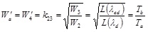
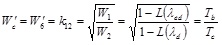
Such a vertical Hall-effect device is shown in Fig. (2). The Hall-effect region is a tub with contacts at its top side. In silicon technology, the tub may be a CMOS n-well, a deeper high-voltage CMOS n-well or an epitaxial layer, and the ohmic contacts are made by shallow n+ source/drain diffusion. We neglect the depth of the contacts and the inhomogeneous doping profile, and we assume a rectangular cross-section of the Hall-tub. Then we can apply our theory to clarify, if it is possible to optimize such devices despite the limitation that all contacts have to be on the top side.
To this end we simply have to find a mapping from the rectangular cross-section of Fig. (2) to the half-plane geometry in Fig. (4b). This is shown in Figs. (15a-c). There we draw a scaled rectangular device in the q-plane and transform it to the t-plane similar to (14a).
 |
(34a) |
The parameter k is given by the aspect ratio of the Hall-tub.
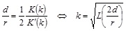 |
(34b) |
d and r are the depth and the length of the rectangular Hall-tub (see Fig. 15a). The mapping of the contacts is
 |
(34c) |
 |
(34d) |
 |
(34e) |
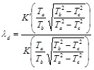
where ra is the length of the center contact, rb is the spacing between center and outer contacts, and rc is the length of the outer contacts (see Fig. 15a). A degenerate Möbius transform
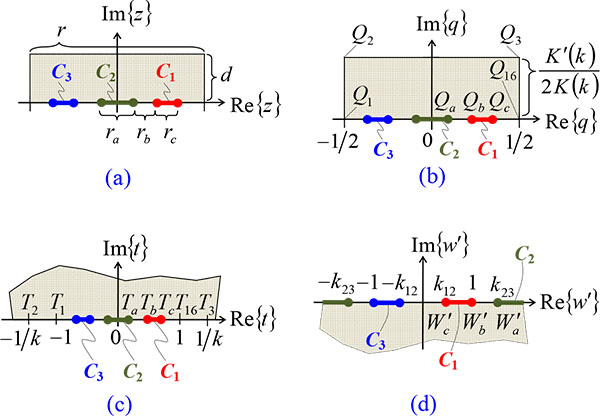 |
Fig. (15). (a) Vertical Hall-effect device with three contacts and single mirror symmetry in the z-plane. (b) The same device in the normalized q-plane. (c) Its conformal transformation on the upper half of the t-plane. (d) Its final transformation on the lower half of the w' -plane: there it is rotated by 180° to Fig. (4b) for Wa' = W4' = k23 and Wc' = W6' = k12 . |
 |
(35a) |
maps the origin onto infinity and vice versa, the upper half of the t-plane onto the lower half of the w' -plane and
 |
(35b) |
 |
(35c) |
 |
(35d) |
Fig. (15d) is rotated by 180° against Fig. (4b), if we set Wa' = W4' = k23 and Wc' = W6' = k12. With (8a,b), (12b) and (19a,b) we get
 |
(36a) |
 |
(36b) |
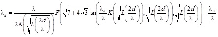
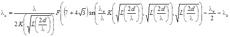
Combining this and solving it, we get the 2 DoF of the layout as functions of geometrical parameters of the Vertical Hall-effect device
 |
(37a) |
 |
(37b) |
With (37a,b) and (34b-e) we can compute the ERC and the Hall-output voltage for any 3C-VHall device from Fig. (2). For maximum SNR at a given impedance level we are looking for electrical symmetry Rd = Re, and even more specifically for the point  on that curve. With (36a,b) this means
 |
(38) |
Summarizing these findings we may assume r, d, ra and derive rb, rc for optimum SNR:
 |
(39a) |
 |
(39b) |
 |
(39c) |
 |
(39d) |
For (39a) we used (34b,c), for (39b) we used (38) and (39a), for (39c) we used (34d) and (39b), and for (39d) we used (34e) and (39c). For real-valued F(w,k) with 0 ≤ k ≤ 1 it must hold 0 ≤ w ≤ 1. Hence, from (39d) we obtain a maximum allowed:
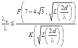 |
(40) |
The meaning of (40) is: if we assume a given aspect ratio d / r of the Hall tub, we can only realize optimized devices (i.e. devices with electrical symmetry and with ) if ra / r is small enough. For practical reasons ra must be larger than the feature size of the semiconductor technology. Fig. (16) shows a plot of the R.H.S. of (40) versus d and r. Obviously, for small d we must use very small ra. For fixed d the length ra can be largest for r → ∞, namely ln(4/3)d/π 0.092d. On the other hand, if one can use the entire chip as Hall-tub, d/r is large, and this means
 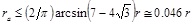 . Thus, even for deep Hall-tubs the length of the center contact must be less than 5% of the device length to achieve - and for shallow Hall-tubs it must be even shorter. With respect to minimum feature size rb and rc are less critical than ra, because from (39c,d) it follows rb > ra and rc > ra. In practice, one should take care that too small ra and rb gives too large electric field, which leads to velocity saturation, electrical non-linearity, temperature gradients and finally to reduced magnetic sensitivity and to poor residual offset at the output of the spinning scheme.
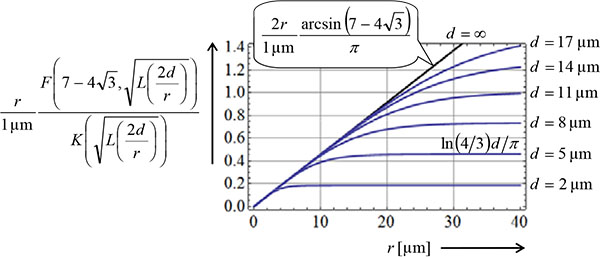 |
Fig. (16).
Minimum required ra of an optimum 3C-VHall device of Fig. (15a) with . For a given depth d and length r of the Hall-tub the length ra of the center contact has to stay below the respective curve (see (40)).
|
For a device with electrical symmetry but with  we have to replace in
  (40) by
  , and this requires even smaller ra/r.
Example:
We aim at a device with length = 20 µm. The Hall-tub is 5 µm deep. With (40) we may choose ra = 0.45 µm and from (39c,d) it follows rb = 0.633548 µm, rc = 6.78451 µm. The results of a finite element (FEM) simulation on this device are shown in Fig. (17). The FEM model used a conductivity of 1 S/m and a sheet resistance of 1 Ω at zero magnetic field. The complete conductivity tensor with the Hall-effect was σxx = σyy = 1 / (1 + (µHB┴)2), σxy = -σyx = µHB┴ / (1 + (µHB┴)2). The mesh had 1.9 million elements and this gave 3.8 million equations. At zero magnetic field the FEM simulation gave a resistance between the outer contacts of 1.154369 Ω (phase 1), and between the center contact and the right contact it was 1.15395 Ω (phase 2). This matches up to 287 ppm and 649 ppm with the analytical formulae (37a,b). Next, the Hall-output voltage was computed for phases 1 and 2 in the limit of vanishing magnetic field. In both cases they agree up to 40 ppm with our analytical formula (31). In both phases the device was supplied by 1 A. Then the Hall-geometry factors are identical up to 0.1 ppm and the supply voltage matches up to 363 ppm for low and high magnetic fields in the range µHB┴ =  0.01, 0.02, 0.05, 0.1, ... ,5.
Please note the usefulness of an analytical treatment in this context. Not only does it prove, that a device with contacts only on one side of the rectangular Hall-region can still have electrical symmetry despite its degenerate geometry – it also shows, that this is possible for all rectangular aspect ratios and what the penalty is, that one has to pay for shallow Hall-tubs. It would have been painstaking to find the optimum of this problem with 4 DoF (ra/r, rb/r, rc/r, d/r) by purely numerical methods.
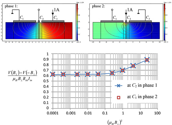 |
Fig. (17).
FEM-simulation of a 3C-VHall-device with d = 5µm, r = 20µm, ra = 0.45µm, rb = 0.633548µm, rc = 6.78451µm operated in phases 1 and 2. In both phases the voltages at the input contacts and the magnetic sensitivities are identical and match with our analytical theory up to better than 649 ppm and 40 ppm, respectively:  , ,  . The color coding denotes the electric potential and the grey lines are current streamlines. . The color coding denotes the electric potential and the grey lines are current streamlines.
|
CONCLUSION
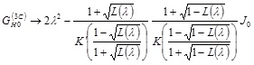
In this paper, we gave an analytical theory of Hall effect devices with three contacts and a single mirror symmetry. This class of devices is of considerable practical relevance, because it includes split-drain MAG-FETs and many Vertical Hall effect devices. The Equivalent Resistor Circuit (ERC) at vanishing magnetic field has three resistors with two different resistance values, but the device geometry has three parameters (two for the layout and one for the thickness). Hence, a 3C-device has 2 electrical DoF and 3 geometrical DoF. As a consequence, one cannot determine the sheet resistance by electrical measurements on a 3C-device. This is a striking contrast to devices with four contacts, whose Hall-output voltage is a unique function of the ERC for fixed input current and Hall angle, whereas the Hall-output voltage of 3C-devices is not defined by the ERC alone – in addition one needs the sheet resistance. We also gave an analytical formula for the weak magnetic field limit of the Hall-geometry factor as a function of the 2 DoFs of the device layout. Various properties of this Hall-geometry factor of 3C-devices were discussed. Numerical values were given in tabular form and some of them were checked by finite element simulations. The maximum signal-to-noise ratio (SNR) at given impedance level is obtained for optimum devices, where the resistance between any two contacts equals  times the sheet resistance. It was also shown that VHalls with three contacts can be optimum for arbitrary depths and lengths of their tubs, however, their center contact has to be smaller than 4.6% of the tub length and smaller than 9.2% of the tub depth.
NOTES
1 Electrical linearity means that the resistance values in the ERC do not depend on the potentials at the various nodes. However, the device may be magnetically nonlinear, which means that the resistance values in the ERC may well depend on the applied magnetic field – so we do not have to limit this discussion to small magnetic fields.
2 The sign of the Hall term originates from the Lorentz force which pulls the electrons to the right hand side of the current streamlines, if the magnetic field points out of the drawing plane. Therefore the Hall electric field points from left to right and consequently the Hall potential at the left hand side of the current streamlines is positive.
3 Meanwhile it was proven rigorously that any Hall device with three contacts and at least one mirror symmetry has the same SNR as its complementary device [30].
COMPETING INTERESTS
The author declares that there are no competing interests.
CONSENT FOR PUBLICATION
Not applicable.
ACKNOWLEDGEMENTS
Declared none.
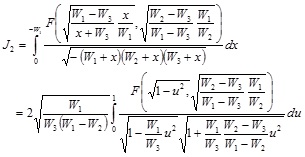
APPENDIX A
Here we compute the integrals in (30). We start with  on the straight line
  . The mapping
  transforms the current density
 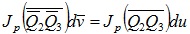 with
with  in the interval 0 ≤ u ≤ 1 (cf. Fig. 8d). Input voltage and current are linked via (17a) Vin = 2λedRshIin. With (16a) we have
  in -1 / kd ≤ ≤ -1 . There it holds
 |
(A1) |
where we used the substitution y = -x. Thus, we get
 |
(A2) |
Next, we change the integration variable du = (du / dt)(dt / dw)dw. For du/dt we use (14a) in the interval 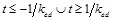 where it holds
 |
(A3) |
 |
(A4) |
Note the minus sign in the numerator at the R.H.S. of (A4), which also becomes obvious from Figs. 8(c, d) . dt / dw is straightforward from (13a). Plugging all this into (A2) gives
 |
(A5) |
with A, C, D from (13b-d) and a,c,d from (15b-d). For the second integral 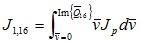 we can use the same
  as above, however this time it is in the interval
  . Inserting W16 = 0 in (15a) gives
  . In this
  -interval it holds
 |
(A6) |
which gives
 |
(A7) |
Here we used the same 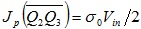 as above, because it is homogeneous in the q-plane. Again we substitute the integration variable du = (du / dt)(dt / dw)dw. For du / dt we use (14a) in the interval -1 ≤ t ≤ 1 where it holds
 |
(A8) |
Inserting all this into (A7) gives
 |
(A9) |
Plugging (A5) and (A9) into (30), we get with (25) in the limit of small magnetic fields
 |
(A10) |
where we used the abbreviation  . With [28, 29] we get
  . The rest of (A10) can be integrated in parts with the same formulae by Prudnikov.
 |
(A11a) |
 |
(A11b) |
 |
(A11c) |
With (19a,b), (14b), (16b), and (B2a,b) we finally get (31).
APPENDIX B
Here we prove = 0 for λed = 0 and for λed = λd.
Inserting λ = λed = λd into (31) gives L(λ) = Led = Ld and
 |
(B1a) |
 |
(B1b) |
Jo is solved by partial integration. With (52a,b) in [22] we have
 |
(B2a) |
 |
(B2b) |
Inserting (B2a,b) into (B1a) gives
 |
(B3) |
With (A17) and (A18) from [5] this leads to
 |
(B4) |
With (19a,b) we see that λed = λd means α1 = α2 = α3. This means that contact C1 touches C2 and contact C3 also touches C2 and the Hall signal disappears.
For λed = 0 we set Led = 1 + dLed with small dLed < 0. We develop the second summand in the integrand in (31) into powers of dLed and integrate. The result goes to  and so it vanishes for λed = 0. The first summand in the integral in (31) can be integrated in parts
 |
(B5) |
The integral at the R.H.S. of (B5) is finite at Led = 1 and  . So the integral in (31) remains finite for λed = 0, but the numerator
  . Therefore it holds
  . With (19c,d) we see that λed = 0 means α1 = 0 while α2, α3 are arbitrary. This means that contacts C1 and C3 touch and the Hall signal disappears.
REFERENCES
| [1] | Wick RF. Solution of the field problem of the germanium gyrator. J Appl Phys 1954; 25: 741-56. |
| [2] | Lippmann HJ, Kuhrt F. Der Geometrieeinfluss auf den Hall-Effekt bei rechteckigen Halbleiterplatten. Z Naturforschg 1958; 13a: 474-83. |
| [3] | Kanda Y, et al. Silicon Hall-effect power IC’s for brushless motors. IEEE Trans Electron Dev 1982; 29(1): 151-4. |
| [4] | Versnel W. The geometrical correction factor for a rectangular Hall plate. J Appl Phys 1982; 53(7): 4980-6. |
| [5] | Ausserlechner U. Van-der-Pauw measurement on devices with four contacts and two orthogonal mirror symmetries. Solid-State Elec 2017; 133: 53-63. |
| [6] | Ausserlechner U. The signal-to-noise ratio and a hidden symmetry of Hall plates. Solid-State Elect 2017; 135: 14-23. |
| [7] | Munter PJA. A low-offset spinning current Hall plate. Sens Actuators A Phys 1990; 21-23: 743-6. |
| [8] | Ausserlechner U. Limits of offset cancellation by the principle of spinning current Hall probe. In: Proc IEEE sensors 2004, Vienna (Austria), 24-27 Oct. 2004; pp. 1117-20. |
| [9] | Stoessel Z, Resch M. Flicker noise and offset suppression in symmetric Hall plates. Sens Actuators A Phys 1993; 37-38(6): 449-52. |
| [10] | Ausserlechner U. Closed form expressions for sheet resistance and mobility from van-der-Pauw measurement on 90° symmetric devices with four arbitrary contacts. Solid-State Elec 2016; 116: 46-55. |
| [11] | Cornils M, Doelle M, Paul O. Sheet Resistance Determination Using Symmetric Sructures With Contacts of Finite Size. IEEE Trans Electron Dev 2007; 54(10): 2756-61. |
| [12] | Ausserlechner U. Two simple formulae for Hall-geometry factor of Hall-plates with 90 degrees symmetry. University Politehnica of Bucharest Sci Bull-Ser A-Appl Math Phys 2016; 78(1): 275-82. |
| [13] | Popovic RS. The vertical Hall-effect device. IEE Electron Device Lett 1984; EDL-5: 357-8. |
| [14] | Stoica D, Motz M. A dual vertical Hall latch with direction detection. In: Proceedings of the ESSCIRC 2013; pp. 213-6. |
| [15] | Sander C, Vecchi MC, Cornils M, Paul O. Ultra-low Offset Vertical Hall Sensor in CMOS Technology. Procedia Eng 2014; 87: 732-5. |
| [16] | Ausserlechner U. Electronic device with ring-connected Hall effect regions. US9007060, July 21, 2011. |
| [17] | Janković N, Pantić D, Batcup S, Igić P. A lateral double-diffused magnetic sensitive metal-oxide-semiconductor field-effect transistor with integrated n-type Hall plate. Appl. Phys. Lett. 2012; 100(26): id. 263507 (4 pages). |
| [18] | Boas RP, Boas HP. Invitation to Complex Analysis. Washington: The Mathematical Association of America, 2010 (2nd ed.), chapter 4, 25. |
| [19] | Ausserlechner U. Hall Effect Devices with Three Terminals: Their Magnetic Sensitivity and Offset Cancellation Scheme. J. Sensors, Hindawi Publ. Corp., 2016, ID 5625607, 16 pages. |
| [20] | Van der Pauw LJ. A method of measuring specific resistivity and Hall effect of discs of arbitrary shape. Philips Res Repts 1958; 13(1): 1-9. |
| [21] | Koppenfels W, Stallmann F. Praxis der Konformen Abbildung. Berlin: Springer Verlag 1959, chapter B.3.1, page 217. |
| [22] | Ausserlechner U. A method to compute the Hall-geometry factor at weak magnetic field in closed analytical form. Electr Eng 2016; 98(3): 189-206. |
| [23] | Weisstein EW. Modular Equation. From MathWorld: A Wolfram Web Resource. http://mathworld.wolfram.com/ModularEquation.html |
| [24] | Versnel W. Analysis of symmetrical van der Pauw structures with finite contacts. Solid-State Electron 1978; 21: 1261-8. |
| [25] | Moon P, Spencer DE. Field Theory for Engineers. Princeton: Van Nostrand Comp.Inc. 1961, chapter 4, sec. 8, §4.08 |
| [26] | De Mey G. An expansion method for calculation of low-frequency Hall effect and magneto-resistance. Radio Electron Eng 1974; 44(6): 321-5. |
| [27] | Moelter MJ, Evans J, Elliott G, Jackson M. Electric potential in the classical Hall effect: An unusual boundary-value problem. Am J Phys 1998; 66(8): 668-77. |
| [28] | Prudnikov AP, Brychkov YA, Marichev OI. Integrals and Series. Vol 1. Gordon and Breach Science Publishers 1986, 1.2.39.1 |
| [29] | Prudnikov AP, Brychkov YA, Marichev OI. Integrals and Series. Vol 1. Gordon and Breach Science Publishers 1986, 1.2.35.1 |
| [30] | Ausserlechner U, Glasser ML, Zhou Y. "Symmetries of certain double integrals related to Hall effect devices." arXiv preprint arXiv:1805.00629 (2018). |